MOSFET -
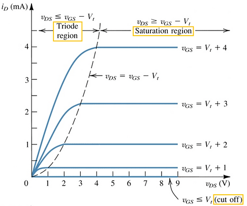
3 OPERATION REGIONS
MOSFET - MOS Field Effect Transistors
This three-terminal semiconductor devices are far more useful than two-terminal ones (ie: diode) because they can be used in a multitude of applications, ranging from signal amplification to digital logic and memory. The basic principle involved is the use of the voltage between two terminals to control the current flowing in the third terminal. In this way a three-terminal device can be used to realize a controlled source.
Metal-Oxide Semiconductor Field Effect Transistor, commonly known as MOS. The transistor is fabricated on a p-type substrate, which is a single-crystal silicon wafer that provide physical support for the device. Two heavily doped n-type regions, indicated in the figure as the n+ source and the n+ drain regions, are created in the substrate. A thin layer of silicon dioxide (SiO2) of thickness tox, which is an excellent electrical insulator, is grown on the surface of the substrate, covering the area between the source and drain regions. Metal is deposited on top of the oxide layer to form the gate electrode of the device. Metal contacts are made to the source region, the drain region, and the substrate, also known as the body.
Thus 4 terminals are brought out:-
a) the source terminal (S)
b) the gate terminal (G)
c) the drain terminal (D)
d) the substrate or body terminal (B)
The Body (B) has no effect on device operation, so the MOSFET is usually treated as a 3 terminal device in most of the circuit analysis.

The insulation causeds the current in the gate terminal to be extremely small.
A voltage applied to the gate controls current flow between source and drain. This current will flow in the longitudianl direction from drain to source in the region labeled "channel region". Two important parameters of the MOSFET, length L and width W.
With no bias voltage applied to the gate, two back-to-back diodes exist in series between drain and source. These back-to-back diodes prevent current conduction from drain to source when a voltage VDS is applied.
Here we grounded the source and the drain and applied a positive voltage to the gate, VGS. When VGS reach a sufficient level, the electrons near the furface of the substrate under the gate induced n-type channel connectiong the source and drain regions. Now the voltage applied between drain and source will create a current flows through this induced channel.
I'm a paragraph. Click here to add your own text and edit me. It's easy.